Project Overview
The goal of the project was to design a circuit that was capable of counting to 80 by using both of the seven segment displays on the breadboard. Other constraints provided that the completed design needed to pause and hold the count on the displays when it reached the value of 80, and the design also needed to incorporate a reset switch built in to clear the displays and begin the entire count again.

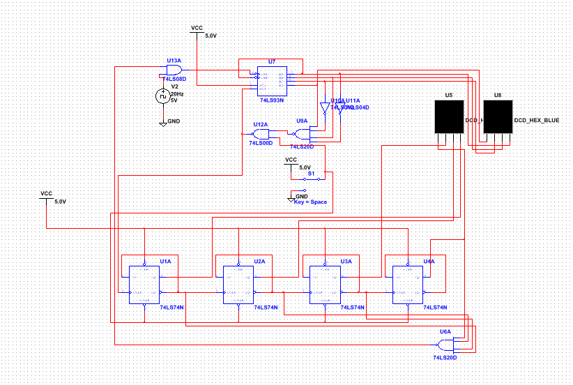
MultiSim Circuit
PLD Circuit
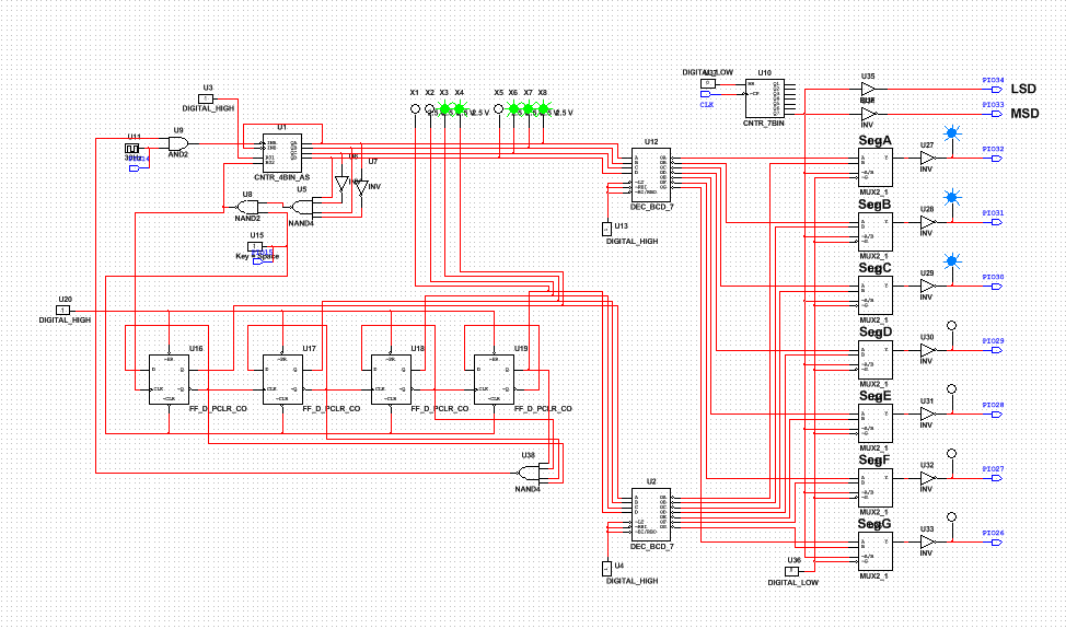
The design mode for multi sim is used to create a working circuit on the computer and also to test different designs to see if they function properly, but the PLD mode is specifically designed to export the circuit to a chip so that it can be tested on a breadboard with real displays and LEDs. The Multi sim and PLD mode uses different labels for the components as the multi sim has numerous types and models of each component, while the PLD mode has generic names so that the general function can be transferred to different types of chips that may use the other models of the components. The PLD mode must also use pins to assign where inputs and outputs will be connected to the circuit so that when the design is implemented the wiring on the circuit board will allow the PLD design to function properly.
Bill of Materials
Materials Quantity
Wires 13
Programmable Chip 1
Breadboard 1
NI myDAQ 1
Wires 13
Programmable Chip 1
Breadboard 1
NI myDAQ 1
Final Project Conclusions
1. The integration of circuitry can be implemented in many sizes and for this project we used SSI (Small Scale Integration) and MSI (Medium Scale Integration). SSI contains 10 or less transistors or logic gates inside of an integrated circuit and is used for smaller deigns like AOI that includes AND, OR, and their various counterparts. MSI contains 10 to 100 transistors per integrated circuit and is used for more complex designs like Flip-Flops and Mulitplexers.
2. The circuit I designed is limited because it could only count up due its use of the 74LS93 chip which has to have its inputs be wired the same in each implementation. Another limitation of the design is the asynchronous clock that is used for the tens counter because the asynchronous design led to a delay in the circuit's display know as the ripple effect.
3. The ripple effect is a delay that occurs in asynchronous counters because the electric signal takes time to travel between the circuits and the clock on each Flip-Flop is based on the output signal received from the preceding Flip-Flop, so each Flip-Flop after the first must wait for the signal to be sent to raise or lower the edge of the clock.
4. The circuit is activated when the reset is powered so that the circuits no longer receive signals to their clears, then the clock's signals are sent to the 74LS93 chip which begins to count from 0 to 9. Each time the circuit reaches 10, a NAND detects the signal and sends a signal out to reset the chip and another signal is sent out to the clock on the tens counter. When the tens counter receives a clock signal it is sent through each Flip-Flop to raise the count by 1, so when the ones counter reaches 9 the next value that is display will increase the tens counter by 1 and reset the ones counter back to 0.
5. Many other classmates took different approaches compared to mine for the circuit because we applied all the lessons we learned recently to the design. Other classmates used different wiring techniques to reset the entire circuit as well as pausing it. Other differences with the design involved the use of different logic gates to do the same job because gates can be used to mimic other gates.
